Disruptive innovation that brings the mobile industry to greater heights.
Introducing
The World First All-Sided Protection Panel Level Chip Scale
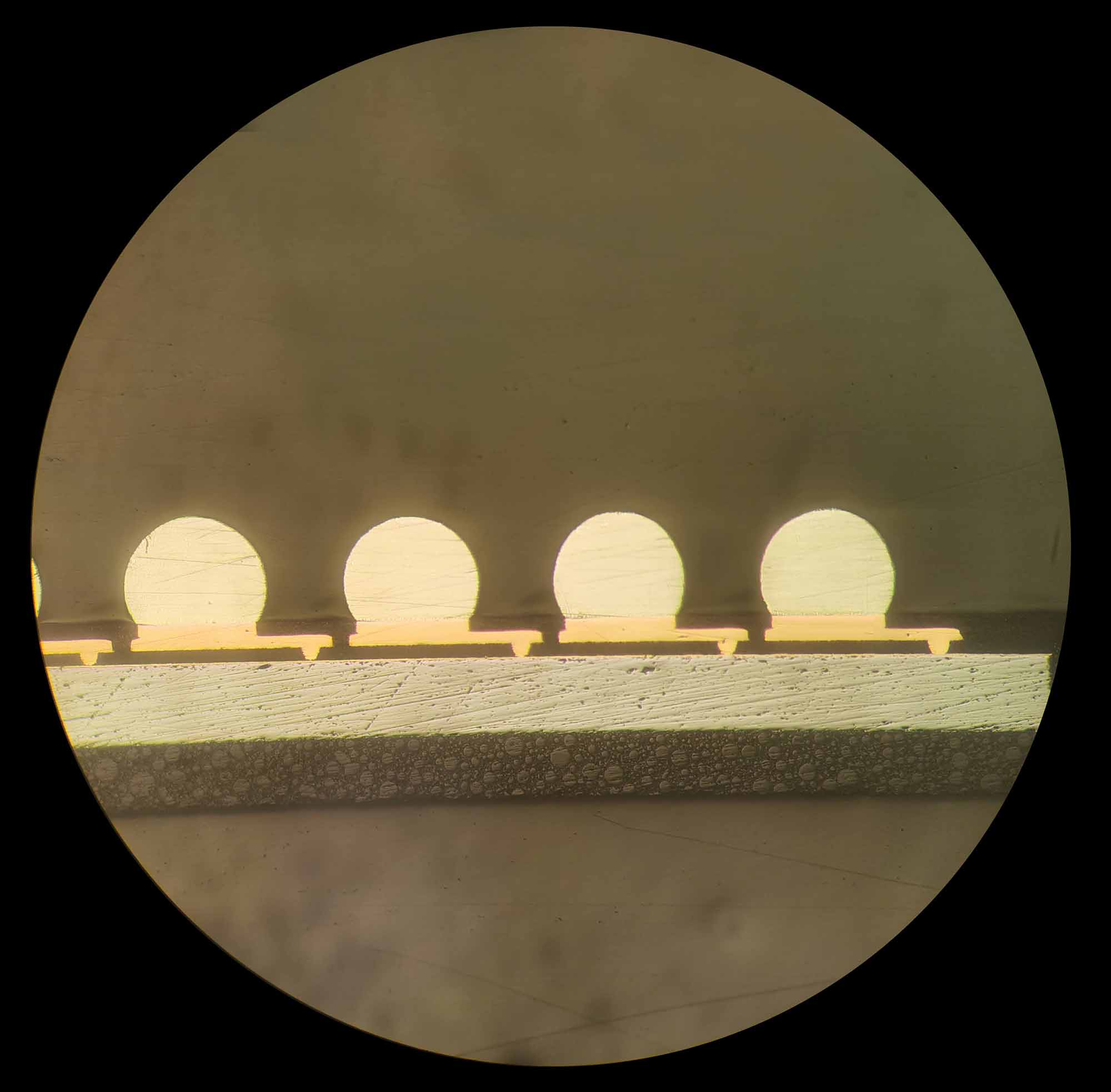
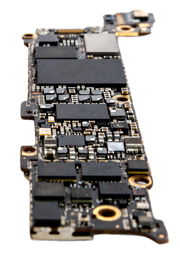
PEP Innovation offers the world first ALL SIDED PROTECTION Chip Scale Package, a high reliability, cost-effective drop-in replacement for existing WLCSP. By virtue of 600 mm X 600 mm Panel level assembly to achieve higher cost efficiency and optimizing material usage, multiple wafers are redistributed with patented precision die placement process, eliminating die shifting problems plaguing the industry. The required circuits are plated and the package encapsulated before singulation to a finished (pin to pin replacement) product
Our mission
“The demands for smaller, lighter packaging solutions whilst keeping sights on high performance in electrical and thermal characteristics have prompted us to push the boundaries of traditional packaging technology in the reduction of cost”
Jimmy ChewChief Executive, PEP Innovation
Innovation
Features
Unique product features overcome varius industry product limitation
Customer Endorsed Quality
Qualified manufacturing processes meet our customers quality expectation
Qualified
Process
Customers qualified processes with docummented process parameters
Qualified Engineering Team
Our team of engineers are ready to answer to any queries
Revolutionizing
the way packaging is done
Thicker dielectric lamination – replacing polymide layer
Thicker RDL Traces for improve current carrying capacity
0.3mm Thin Package – aligning with market trend
Molded compound protection on all sides to reduce backside chipping and handling damage
Cost reduction on Panel level assembly
Thick copper studs protect circuitry from solder electromigration