Design rules
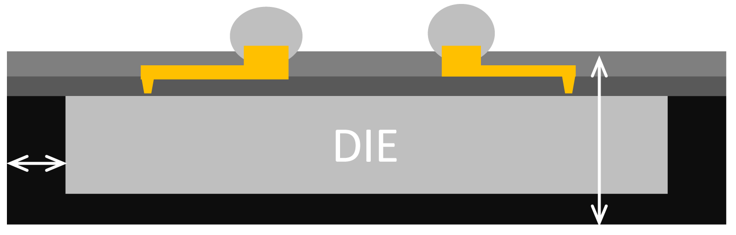
1st Die electric thickness (ABF)
Thickness (µm):
Min: 20
Max: 40
TOL.(µm): 7
RDL Line – Space
Thickness (µm): 20µm-20µm TOL.(µm): 7
RDL Cu trace thickness *
Thickness (µm):
Min: 15
Max: 25
TOL.(µm): 15%
Stud Cu (Bump) thickness
Thickness (µm):
Min: 15
Max: 25
TOL.(µm): Ref.
2nd Die electric thickness (ABF)
Thickness (µm):
Min: 30
Max: 50
TOL.(µm): 15
Silicon die thickness
Thickness (µm):
Min: 150
Max: 725
TOL.(µm): 20
Die back mold compound
Thickness (µm):
Min: 100
Max: 185
TOL.(µm): 20
Pkg thickness
(exclude ball)
Thickness (µm):
Min: 300
Max: 1000
TOL.(µm): 40
EMC side wall thickness
Thickness (µm):
Min: 50
Max: —
TOL.(µm): +/-5
Component Level Reliability Data.
Moisture Sensitivity Level
MSL1, (260°C, 3x)
Temperature Cycling after Precon
-65°C/150°C, 1000 cycles
Unbiased HAST after Precon
130°C/85% RH, 192 hrs
High Temperature Storage
150°C, 1000 hrs
Temperature Humidity Bias Test
85°C/85%/5V, 1000 hrs
Ball Shear Test
Post reflow: T0, 5X and 10X reflow: 260 +0/-5 °C
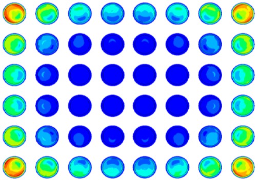
Standard WLCSP
Side and corner bump illustrate a yellowish to reddish colour, highlighting the stress on the corner joints. Over time, the CTE mismatch of the silicon (die) and the PCB create stress in the solder connection. This result in a deterioration of the solder ball reducing the lifespan of the package.
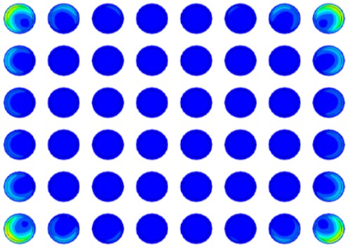
PEP Innovation Protected PLCSP
PEP panel level CSP has a tall copper tower holding the solder ball, creating a stress buffer against elevated current density and electromigration enhancing the lifespan of the package.
Simulation data shows 2 times longer solder life time.
For thermal cycling, the critical joint is at the corner bump, which is the furthest bump location from the neutral point, the package center. The strain energy-density-distribution (SED) for the corner bump at the bump-UBM pad interface can be used to predict the thermal cycle lifetime of the part.