Through years of research and development by a team of highly qualified engineers, PEP innovation is proud to acquire a set of specialized know-how and and patent that govern how we build a semiconductor packages that meets the requirement of our customers, in and outside the silicon valley
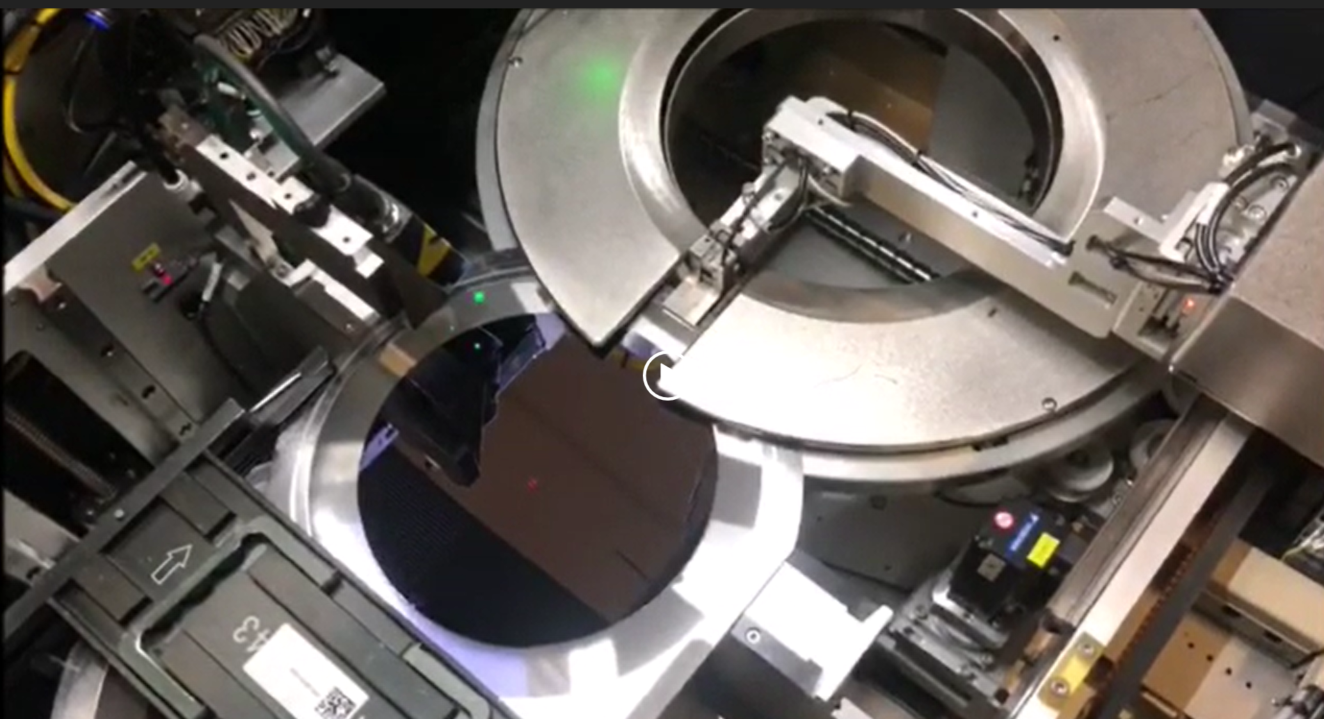
From the incoming shipment from our customers, the wafers are handled with the strictest protocol. WIP go through our qualified processes to ensure finished products are aligned with specification and achieving super high yield synonymous with wafer level processing.