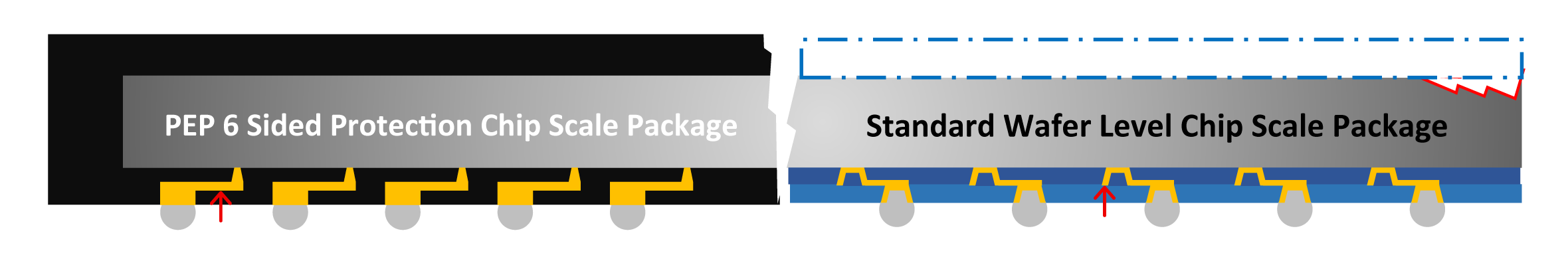
PEP Innovation Unique Features Vs WLCSP
Introducing
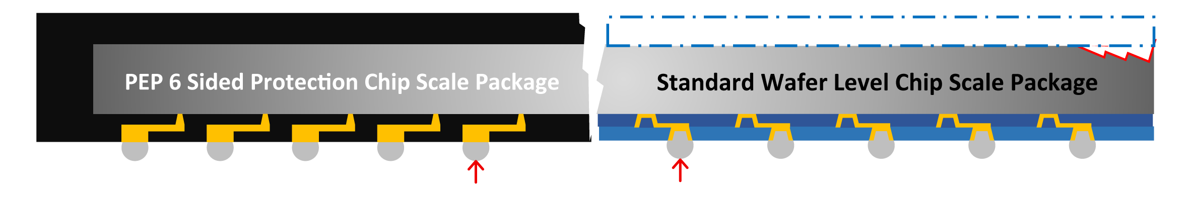
PEP Innovation First All-Sided
Protection Panel Level Chip Scale Package
Protect your package against electromigration in solder joint with thick Cu stud!. Robust outer lead improve drop test reliability and 2x solder life time
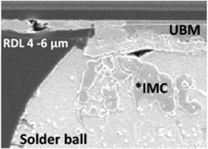
Potential risk of electromigration in solder joint
Electromigration damage was observed along with accelerated diffusion and intermetallic compound growth at the solder (UBM) interface
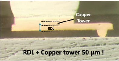
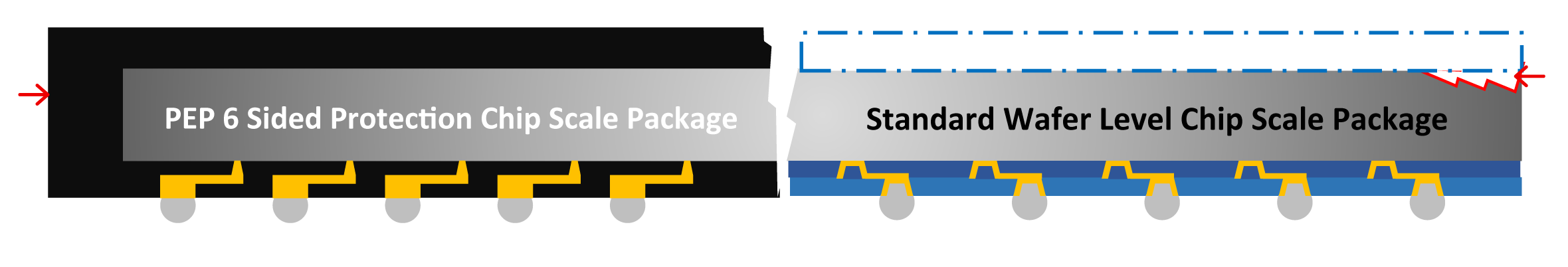
Thick copper traces in redistribution layer Lower RDS(on)
Thinner copper RDL restricted by standard industry design rules
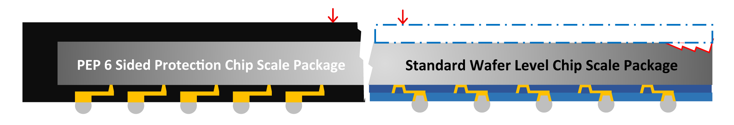
Potential risk of Electrical failure
Failure can occur due to an open in RDL with higher temperature, high current density, and reduced RDL trace width.
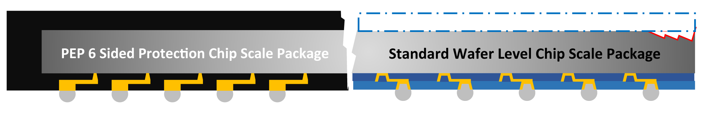
6 Sided Protection, No exposed die surface
With PEP 6 sided protected CSP, transistors diodes and ICs are encapsulated in opaque housing greatly reducing the risk of damange and malfunctions.
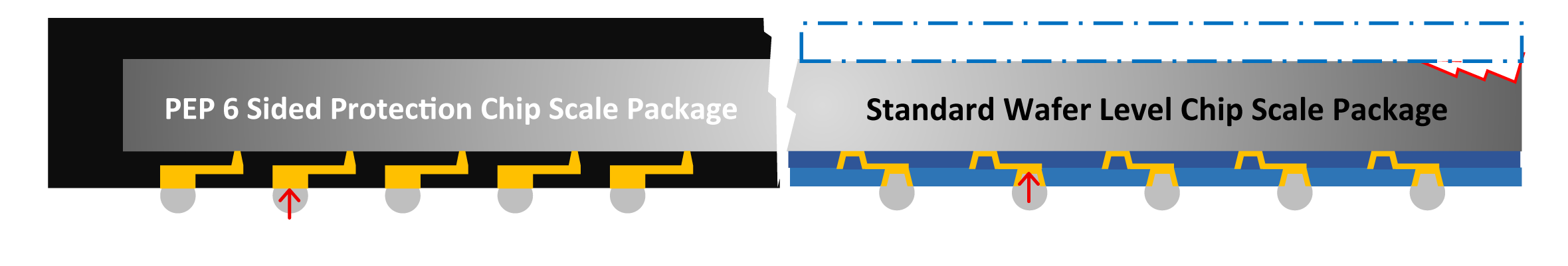
Exposed top and side wall increase the risk of die chipping and unwanted photodiode effect
Semiconductors contain P-N junctions and can fail when exposed to electromagnetic radiation (light) of wavelength producing a photocurrent.
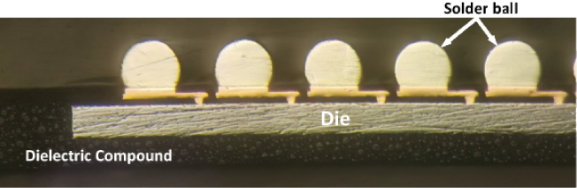
Homogenous use of Dielectric for superior warpage management
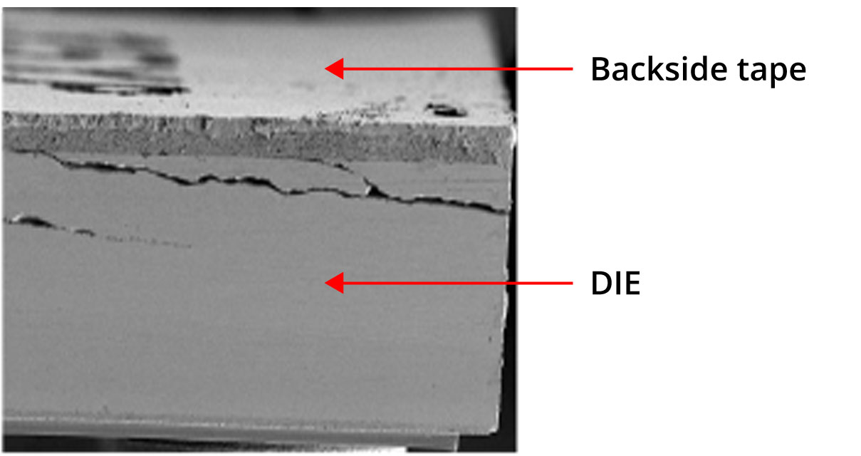
Defect in a backside coated package
Die crack is hidden by the backside coating. There is no good way to screen damaged parts as side wall inspection has a large impact on efficiency and cost.
Pin to Pin Compatibility
Drop in replacement shorten qualification